Unknown Nanostructures Give Up Secrets to Interdisciplinary Group at LBNL
August 7, 2007
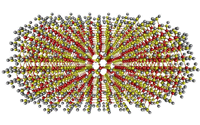
Calculated dipole moment of a 2633-atom cadmium selenide quantum rod, Cd961Se724H948. The computation, performed on 2560 processors of the Seaborg computer at the National Energy Research Scientific Computing Center at Lawrence Berkeley National Lab, took about 30 hours. Effects of the dipole moment and internal electric field of a nanostructure are needed for an accurate description of the electronic and optical properties of the structure.
Michelle Sipics
Nanomaterials and devices have generated a media storm in recent years, with scientists touting potential applications in computing, communication, and medicine, among other fields. Articles envisioning therapeutic "nanobots"---tiny robots that could one day travel through the bloodstream to deliver medicine---have garnered serious attention, as have related stories about devices capable of detecting dangerous chemicals in the air or diseases in the human body.
Most of these devices are still a way off, however, with various technical hurdles to be overcome. One of those hurdles involves fabrication of the devices. Nanomaterials can be created in a laboratory environment, but the process includes an element of randomness: Researchers cannot determine at the outset exactly what structure they will get. Not only are they unable to produce exactly what they want---even when a structure is complete, they can't say exactly what they've produced, or what it can do.
Among the many scientists working to advance the field are Juan Meza and colleagues at the Department of Energy's Lawrence Berkeley National Laboratory. "Our group has been involved in materials sciences calculations for quite a few years," says Meza. The group's most recent efforts have been part of a joint initiative of two DOE offices, Basic Energy Sciences and Advanced Scientific Computing Research.
On the scale of billionths of a meter, the smaller-than-microscopic but larger-than-molecular nanostructures have become the subject of numerous enormous research projects. In the 2006 federal budget process, President Bush requested more than $1 billion for nanotechnology research. DOE's share in the National Nanotechnology Initiative grew from $231 million in 2006 to an estimated $293 million in 2007. The goal of the DOE initiative, Meza says, "was to bring together scientists from chemistry and materials sciences and mathematics and computer science" to speed progress in nanotechnology. By collaborating with people from areas of study other than their own, the Lawrence Berkeley scientists have obtained promising results---including a new solution to the problem of identifying unknown structures.
"Inside a nanostructure, for example a quantum dot, the atoms arrange themselves quite nicely into a crystal structure," Meza explains. When it comes to the overall shape and size of the structure, though, an element of randomness creeps in. "The size in particular is interesting," he points out, "be-cause different sized quantum dots can give you quite different properties."
It is a structure's surface, however, that poses the greatest difficulty. "The surface is harder to figure out because of the interaction with the �outside world,'" Meza ex-plains. "Depending on what the nanostructure is in contact with, the surface could look very different."
The trick is to minimize the potential for interaction with the outside environment as much as possible, as with a group of young children you're trying to get to sit still for a picture. If you turned them loose in a room with dozens of toys, they would most likely end up running in all directions trying to grab the items they wanted to play with. But if you sat them at desks and gave each child the same toy to play with---something simple that could hold their attention for a little while---they just might sit still long enough for a quick photograph.
Meza and his group use a similar technique---called "passivation"---to keep nanostructures on their best behavior. Usually, they accomplish this with hydrogen atoms: With a single electron each, hydrogen atoms attach to atoms on the surface of a nanostructure, preventing them from moving too much without disturbing the rest of the structure. That paves the way for the final step in the identification of an unknown nanostructure: ground-state calculations.
Any material has a unique "ground state"---that is, the minimum-energy level where the material's electrons remain unless the material is perturbed by external sources. "We are interested in the electron density associated with this level," says Chao Yang, a member of Meza's group from the Computational Research division of LBNL.
If it is possible to determine a material's ground state, it is possible to identify the material itself--much as human beings can be identified by their fingerprints. Unlike law enforcement agencies, however, scientists currently have no way to take a quick snapshot of a material's electrons and compare a map of their locations to entries in a database.
"One cannot talk about the exact trajectory of an electron," Yang says. Using a density function, however, it is possible to describe the probability of finding an electron in a certain place.
With a brute-force approach to solve the relevant many-body Schr�dinger equation, ground-state calculations require huge computational resources. To reduce the computational cost, researchers in chemistry and physics developed a reductionist approach, essentially focusing on one electron at a time, and generating nonlinear eigenvalue problems in the process. The electrons' motion can be represented by a set of single-electron wavefunctions---denoting orbitals---giving the researchers an opportunity to identify a material by its ground state. This approach has been used for many years, although it too is problematic, given the difficulty of solving nonlinear eigenvalue problems. (Yang gave a talk at the 2005 SIAM Annual Meeting on his work with LBNL colleagues Meza and Ling-wang Wang in which he discussed the problems posed by nonlinear eigenvalue problems in electronic structure calculations; see SIAM News, April 2006, page 12, www.siam.org/news/news.php?id=931.)
The self-consistent field method---one technique for solving the equations in question---is not always adequate.
"The problem with SCF is that it may not converge---and even when it does, the total energy may not decrease monotonically throughout the iterations," Yang explains. "The reason is that SCF does not try to minimize the total energy directly.
"We view the SCF iteration as a way to seek the minimizer of the total energy indirectly, by minimizing a sequence of quadratic surrogate functions," he says. "Each surrogate function is constructed by matching the gradient of the total energy at the current approximation. However, if we move along a descent direction associated with the surrogate function, there is no guarantee that the true total energy will decrease."
In other words, even when SCF ultimately converges, the total energy from one SCF iteration to the next can actually increase.
The LBNL researchers had an idea about how to improve on SCF: minimize the total energy directly. Their approach, termed "direct constrained minimization," breaks the problem up, projecting the total energy function into a sequence of overlapping subspaces of small dimensions. It then seeks the minimum of the projected total energy within each subspace. Each solution produces an optimal step length and search direction---simultaneously. An additional constraint is added to ensure that the total energy decreases monotonically.
The net result? The physical properties of unknown nanostructures can now be identified more quickly than before. In the future, the researchers add, experimentalists may be able to create structures designed for a specific purpose.
"We can find the relationship between the shape and chemical components of the nanocrystal and these physical properties, then ask the experimentalists to synthesize the corresponding nanocrystals," Wang explains. "The experimentalists are getting very good at synthesizing different shapes of nanocrystals."
"The more we can compute about a particular application, the better idea we have about the use of certain materials in various applications," adds Meza. "That can cut down tremendously the amount of time that an experimentalist needs to try out new combinations of materials, and help him decide how to prioritize the set of experiments he wants to do by telling him which ones are the most promising."
Meza credits the interdisciplinary atmosphere of the project as fundamental to the group's success. "As a result of this project, we've been able to work closely with people outside our fields and get a better understanding of the underlying problems, which has led to several new approaches, one of which is a new linear scaling approach for electronic structure calculations---but that's another story," he says.
The group hopes to develop additional new algorithms so that they can study ever-larger problems.
"With these new computational capabilities," Meza says, "we should be able to answer questions about some of the results that have puzzled experimentalists for quite a number of years."
Michelle Sipics is a contributing editor at SIAM News.
![]()